FDC Pat Gelsinger wishes to make Intel the world’s second biggest chip producer by 2030, which indicates serving organizations the x86 giant has actually typically viewed as rivals.
“We wish to be the foundry for the world. If we’re going to be the Western foundry at scale, we can’t be discriminating in who’s taking part in that,” he stated throughout Intel’s Foundry Direct Connect occasion in San Jose, California Wednesday.
To do this, Gelsinger is splitting the chip store down the middle, to form 2 independent companies under the Intel brand name. As part of the reorganization and rebrand, Intel Foundry Services will be broadened to consist of the chipmaker’s innovation advancement, supply chains, fabrication, and product packaging services under the IFS name.
Intel’s Product department will focus its efforts on advancement and licensing customer, desktop, and networking set. In result, this Intel items arm will operate more like a fabless chipmaker than it has formerly.
These companies will be lawfully unique and have their own personnel and procedures with very little overlap to make sure privacy, described IFS head Stu Pann.
“We’re extremely disciplined about this. We have 2 different sales forces. We’re constructing 2 different ERP systems. We’re describing 2 different legal entities,” he stated. “Intel Foundry will do arm’s length deals with the Product groups.”
The Product group will likewise get fabulous allowances– which he described as capability passages– the like any other consumer. He did confess that Intel Products would likely drive the bulk of Intel’s organization for the next number of years.
Possibly more significantly, Intel Foundry will preserve stringent privacy with each of its consumers– despite whether they’re internal or external. “This is at the heart of what it requires effective in foundries,” Intel EVP of producing Keyvan Esfarjani discussed.
‘Strange bedfellows’
While Intel has legal structures in location to separate the Foundry and Product departments, the method is currently playing out with Intel’s collaboration with Arm.
Arm is working to make its copyright offered on Chipzilla’s procedure nodes. Faraday is currently revealing chips utilizing both of their innovations.
- Intel hold-ups Ohio fab develop, blames semiconductor downturn
- Sam Altman’s chip aspirations might be loonier than feared
- GlobalFoundries ratings $1.5 B in Uncle Sam’s semiconductor aid treasure trove
- Arm targets AI efficiency with most current Neoverse Compute Subsystems
The unconventional nature of the collaboration wasn’t lost on Arm CEO Rene Haas, who, signing up with Pann on phase, explained the coupling as “unusual bedfellows.”
“I was attempting to think about a parallel appropriate to this story and the only thing I can think about is, for those who can harken back, is when Walt Mossberg asked Steve Jobs what it resembled to see iTunes working on Windows? I believe he stated it resembled ice water in hell, however I will not go that far,” Haas stated.
The foundry group’s goal is to fill the fabs. We hope that consists of Jensen and Cristiano, and Sundar, and you heard today it consists of Satya, and I even hope that consists of Lisa moving forward,
Along With Arm, Gelsinger talked up its tactical collaborations with chip style business like Cadence, Ansys, Siemens, and Synopsys, and promoted an agreement from Microsoft to develop chips on its 18A procedure node. Microsoft– a relative beginner to custom-made silicon– is just the idea of the iceberg for Gelsigner’s aspiration.
“The foundry group’s goal is to fill the fabs. We hope that consists of Jensen and Cristiano, and Sundar, and you heard today it consists of Satya, and I even hope that consists of Lisa moving forward,” he stated, noting off executives from Nvidia, Qualcomm, Google, Microsoft, and AMD.
While Intel is trying to preempt any disputes of interest through this reorganization, Gelsinger does not appear to be all set to provide up the secrets to the kingdom and spin off its foundry organization as a standalone entity.
That stated, the spinoff of Intel’s programmable services group in 2015 recommends that the exact same might occur as soon as Intel Foundry is more developed.
Intel plots course for brand-new procedure tech
Obviously, drawing in significant chip suppliers like Nvidia or AMD initially needs having a procedure and product packaging tech worth the threat.
Intel teased the follower to its 18A procedure node called 14A, which will be its very first produced utilizing ASML’s High-NA EUV lithography devices– Click to increase the size of
To this end, Intel teased its next-gen procedure tech which, from the roadmap, must begin presenting in between 2025 and 2027. Amongst the nodes is a follower to the unreleased 18A procedure node called Intel 14A, which will be its very first to utilize ASML’s High-NA extreme-ultraviolet lithography tech.
There are in fact 2 procedure nodes based upon the tech: 14A and a boosted variation called 14A-E, which will most likely come later on. In addition to the procedure diminish, Intel likewise prepares to present a performance-optimized variation of its 18A node, naturally called 18A-P along with improved variations of its older procedure nodes consisting of Intel 3-E and Intel 3-PT.
The latter is an efficiency enhanced procedure node created with through-silicon VIAs for applications utilizing 3D product packaging. Intel prepares to put this tech to deal with its next-gen many-cored CPU code word Clearwater Forest.
We do not understand much about the chip right now, however we do understand it will stack CPU tiles constructed on Intel 18A on top of a provider tile based upon Intel 3. We’ve seen a comparable strategy utilized on AMD’s MI300A APUs, though the product packaging tech is a bit various.
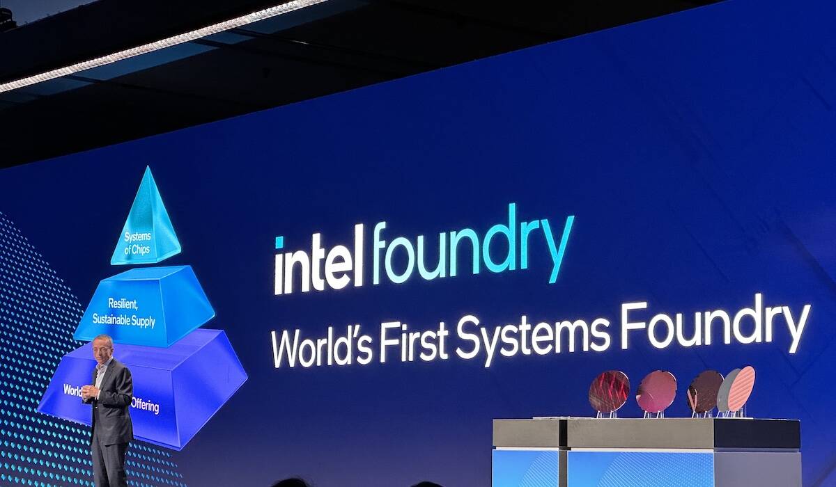
Intel thinks this procedure tech, together with worldwide dispersed and sustainable fabs, will form the basis of what Gelsinger called a “systems foundry.”
The concept appears to be that Intel will offer more than simply making and product packaging services like TSMC. Rather it will guarantee to offer other worth contributes to support more complicated heterogeneous chiplet styles utilizing internally and externally sourced copyright.
Still waiting
United States commerce secretary Gina Raimondo didn’t have any CHIPS fund surprises for Pat Gelsinger throughout her IFS Direct Connect look, however stated a 2nd CHIPS expense wasn’t out of the concern– Click to expand
Considering that Gelsinger initially revealed Intel would open its foundries to agreement production in 2021, the chipmaker has actually devoted to developing more than $100 billion worth of chip factories throughout the United States and Europe.
Much of this work, nevertheless, depends upon significant federal government aids under the United States and EU CHIPS Bills. Regardless of Global Foundry’s $1.5 billion award Monday and commerce secretary Gina Raimondo’s virtual look throughout Wednesday’s keynote, Intel is still waiting on its piece of the pie.
The wait might yet deserve it. As we just recently found outIntel might get as much as $10 billion in aids from the $39 billion reserved for fabulous tasks. And as we’ve formerly reportedthat number might wind up being even greater.
On the intense side– for Intel a minimum of– there might be much more financing on the horizon. When inquired about the possibility of a 2nd CHIPS costs, Raimondo didn’t nix the concept. “I presume there will need to be … CHIPS 2 or something else … ongoing financial investment … if we wish to lead the world,” she responded.
As enticing a possibility as CHIPS money might be, the speed or absence thereof with which the very first expense has actually been distributed has actually currently triggered concerns for Intel’s fabulous construct out. Previously this month, it was reported that Intel had actually postponed its Ohio foundry task to 2026 due to the weak semiconductor market and hold-ups in getting CHIPS Act aid money. ®