Serving the tech lover neighborhood for over 25 years.
TechSpot suggests tech analysis and recommendations you can rely onRead our principles declaration
In quick: As generative AI demolishes increasingly more capability, the advancement of high-bandwidth memory items will be essential to its ongoing performance. Providers are presenting 2nd generation HBM3 items however genuine modification will feature HBM4.
SK Hynix’s most recent high-bandwidth memory item, HBM3E, is presently in mass production and will be presented into the marketplace in the very first half of this year, according to remarks vice president Kim Chun-hwan made throughout his keynote speech at SEMICON Korea 2024 recently. By 2026 the business anticipates that it will be standardizing HBM4, its 6th generation HBM, he included.
Kim likewise supplied info about the business’s DRAM and NAND flash items. It is presently mass-producing 1b-level circuit line width items and establishing 1c, which represents the next generation, he stated. SK Hynix prepares for “extreme technological constraints” listed below the 10-nanometer level and for that factor the business is pursuing the advancement of brand-new products and structures.
The quick development of generative AI is moving need for these memory items, with Kim keeping in mind that the generative AI market is anticipated to grow at a yearly rate of 35%. In specific, high-bandwidth memory– very first presented to the marketplace in 2013 amidst cautions that it would never ever end up being commercially feasible– enables the lightning-fast information transfers required for numerous of these applications. Simply to mention one example, Micron Technology boasts that its HBM3 Gen2 memory with bandwidth higher than 1.2 TB/s and pin speed over 9.2 Gb/s decrease training times of big language designs like GPT-4. Efficiency, in other words, has actually taken off.
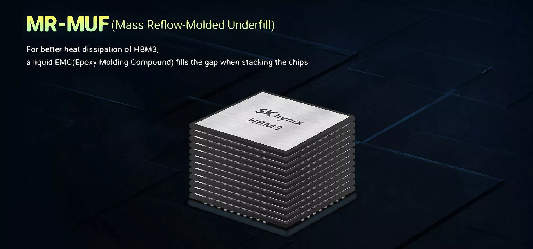
The very first model of high-bandwidth memory was rather restricted, just enabling speeds of as much as 128 GB/s per stack. HBM2 doubled possible speeds to 256 GB/s per stack and optimal capability to 8 GB. In 2018, HBM2 got an upgrade called HBM2E, which even more increased capability limitations to 24 GB and brought another speed boost, ultimately striking 460 GB/s per chip at its peak. The speed doubled once again with the rollout of HBM3, to an optimum 819 GB/s per stack while abilities increased to 64 GB. Came another upgrade, HBM3E, which increased theoretical speeds up to 1.2 TB/s per stack.
Throughout this history, HBM kept the exact same 1024-bit per stack user interface– a specifying quality of the innovation. That will alter with HBM4, anticipated to have a 2048-bit user interface that might in theory double transfer speeds once again, presuming producers are able to preserve the very same transfer rates, a task that is in doubt.
As specs for HBM develop, so does the marketplace itself. Trendforce reported in 2015 that Nvidia prepares to diversify its HBM providers for more robust and effective supply chain management. It likewise anticipated a considerable shift towards modification need in the HBM4 market, moving far from the standardized method of product DRAM. This approach modification is anticipated to cause special style and rates methods, Trendforce stated, and introduce an age of specific production in HBM innovation.