
High throughput and high accuracy can help in reducing solar battery production expenses. A research study group at Fraunhofer ISE has actually made development with a laser system to procedure wafers for metallization. The system supposedly works 10 to 20 times much faster.
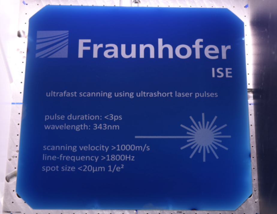
Image: Fraunhofer ISE
With a brand-new kind of laser, wafers can be processed 10 to 20 times faster than in the past. This is the outcome of a research study job at the Fraunhofer Institute for Solar Energy Systems (Fraunhofer ISE) in Germany.
The scientists established a model that can inscribe the finest structures in silicon wafers utilizing UV waves. The brand-new system principle makes it possible for solar battery producers to perform laser processing at the greatest speed without needing to jeopardize on the size of the structure or processing field.
In order to produce solar batteries from wafers, the wafers must, to name a few things, be metalized. Throughout this action, fine channels are furrowed on the top of the cells. The silver paste enters into the channels and after that functions as a conductor track. The speed at which the channels come onto the wafer is really essential for the production of cells to even more lower production expenses.
The laser provided by Fraunhofer ISE can draw 1800 lines per second. This is 10 to 20 times as quick as a so-called galvanometer scanner, which is frequently utilized for this function. The laser has a high repeating rate of 10 megahertz and an optimum pulse energy of 5.6 microjoules.
Popular material
The laser can likewise process wafers in M12 format with a side length of 210 millimeters. The channels inscribed by the laser are simply 15 micrometers large. This is 30 percent finer than present UV wave lasers that are currently utilized commercially. Compared to the very prevalent infrared lasers, the channels of the brand-new laser are 3 times as fine. Finer channels enable decreased usage of silver paste and can hence assist even more decrease production expenses.
“The unique feature of the style of the demonstrator is that big workpieces can be processed really rapidly and with a little structure size,” stated Jale Schneider, task supervisor at Fraunhofer ISE. “A big image field, quick processing, great structures– the concept that you can just have 2 of these 3 residential or commercial properties at the very same time is securely anchored in the laser product processing market. With this system, we have actually satisfied all 3 dreams at the very same time.”
German laser expert Edgewave GmbH established the model. Moewe Optical Solutions constructed a polygon scanner for the job. At Fraunhofer ISE, the group created the polygon scanner, the laser and an axis for beam assistance into a system. The group now wishes to take a look at brand-new procedures to increase throughput.
This material is secured by copyright and might not be recycled. If you wish to work together with us and wish to recycle a few of our material, please contact: editors@pv-magazine.com